Intel's Atom Architecture: The Journey Begins
by Anand Lal Shimpi on April 2, 2008 12:05 AM EST- Posted in
- CPUs
2-Issue and In-Order: Intel's Version of the Cell's PPE
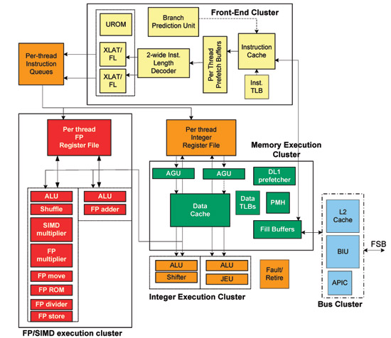
The Austin design team started with a single-issue in-order core but quickly expanded it to be a superscalar, 2-issue design, in other words it is capable of sending up to two instructions down the pipeline at the same time. By comparison most desktop x86 microprocessors are 3 or 4-issue designs.

In order to feed the 2-issue machine, Intel equipped Atom with two decoders. These decoders take instructions fetched from the L1 instruction cache and sequence the series of 1s and 0s into figuring out what the instructions are telling the CPU to do. While the decoders are equal in their ability to decode instructions, there are two paths that an instruction may take: slow and fast.
In the earlier days of the x86 ISA (Instruction Set Architecture) many complained about its support for variable length instructions.
If I tell you that I'm going to give you 2 oranges every 10 seconds, your job becomes much easier than if I tell you that I'm going to give you somewhere between 1 and 3 oranges every 10 seconds. The former would be an example of a fixed length instruction set and the latter a variable length instruction set, unfortunately x86 falls into the realm of the latter.
Atom's slow decoding path does not include any speculative decoding. The instructions are sequenced manually, meaning that each bit is looked at (which takes time) but the instruction is guaranteed to be decoded properly. The instruction is also tagged so that the next time it comes through it can be sent through the fast path.
The fast path obviously employs some speculative decoding and is aided by the tag bit that's set after an instruction goes through the slow path. The slow path yields 1 instruction every 3 clocks, while the fast path can produce 2 instructions every clock.
As Intel learned with Banias (Pentium M), the power penalty for incorrect speculation is unacceptable in a device running on a battery. You'll see a number of tradeoffs where speculative performance tricks are sacrificed in order to maintain low power operation with the Atom processor.


46 Comments
View All Comments
lopri - Thursday, April 3, 2008 - link
This article is as much propagana-ish as it is technical. Did you read the last page of the article?clnee55 - Friday, April 4, 2008 - link
Since Anand wrote this article. I let him answer your accusationGulWestfale - Wednesday, April 2, 2008 - link
i believe that the graphics core in the chipset is a powerVR gen5 derivative; intel already uses some of their tech in its existing mainboards and wikipedia states that intel has licensed gen5 tech for one of its chipsets, the GMA500 (which is the same as poulsbo?) gen5 is also DX10-capable, which matches the info in your article.http://en.wikipedia.org/wiki/PowerVR#Series_5_.28S...">http://en.wikipedia.org/wiki/PowerVR#Series_5_.28S...
yyrkoon - Wednesday, April 2, 2008 - link
and wikipedia has been known to be wrong . . . a lot lately it seems.My point here *is*, I would probably trust anandtech more than wikipedia now days, as it seems any Joe can put up a 'reference' without citation.
jones377 - Wednesday, April 2, 2008 - link
Following the references link from the Wiki article...http://www.imgtec.com/News/Release/index.asp?NewsI...">http://www.imgtec.com/News/Release/index.asp?NewsI...
Poulsbo uses a PowerVR 3D core
Anand Lal Shimpi - Wednesday, April 2, 2008 - link
Yep, you guys are correct, I wasn't aware that it was public yet :) I've updated the article.Take care,
Anand