FIRST LOOK: ULi M1697 for Athlon 64/x2
by Wesley Fink on December 13, 2005 12:05 AM EST- Posted in
- CPUs
Basic Features: ULi M1697 Single Chip
The ULi Award BIOS provides a typical range of BIOS control options for a Reference Board used to qualify a chipset. The wide 200 to 400 range for CPU clock was a pleasant surprise, but it is somewhat academic with no memory voltage controls present in the BIOS. The memory tweaking adjustments were extensive, but of limited use without some means of controlling memory voltage. Reference Boards demonstrate chipset features and capabilities to manufacturers, and ULi clearly shows that the M1697 is capable of supporting whatever range of BIOS control or Voltage control features that the manufacturer might wish to implement.
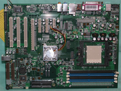
The M1697 is not a board that will be mistaken for a production motherboard. You can see CNR and other risers in odd locations, 4 USB 2.0 ports on the bottom, and a range of PCIe slots that can be turned on or off to test various configurations. Reference Boards are distributed by chipset makers for qualification and not for production. It would therefore be a mistake to dwell on the Reference Board layout, except to say that Reference Boards often influence layout of production boards. IDE, SATA, video slots and bottom edge headers all work fine where they are located. However, we hope that production boards will take a different approach to the location of the 24-pin ATX power connector. Located in about the center of the board between the CPU and rear IO ports, there is really no good way to route the heavy cable. In the center of the board, you have to be careful not to interfere with air flow or operation of the CPU and memory.
The location of the floppy connector at the bottom of the board will be a long reach for floppy users. Many buyers don’t care about floppies any more, but if you still use them, the bottom of the board is an inconvenient and hard to reach location.
| ULi M1697 | |
| CPU Interface | Socket 939 Athlon 64 |
| Chipset | ULi M1697 Single-Chip |
| Bus Speeds | 200 to 400MHz in 1MHz Increments |
| PCIe Speeds | 100-125MHz in 1MHz Increments |
| PCI/AGP | Fixed at 33/66 |
| AMD K8 Cool'n'Quiet | Auto, Disable |
| Core Voltage | Startup, 0.825V to 1.55V in 0.025V increments |
| CPU Clock Multiplier | Startup, 4x-25x in 1X increments |
| HyperTransport Frequency | 1000MHz (1GHz) |
| HyperTransport Multiplier | 200, 400, 600, 800, 1000, Auto |
| DRAM Voltage | Provision for 2.62V, 2.72V (Not implemented) |
| HyperTransport Voltage | 1.20, 1.25, 1.30, 1.35, 1.40V by DIP Switch |
| Chipset Voltage | 1.80 to 2.2V in .05V increments by DIP Switch |
| PCIe Voltage | 1.80 to 2.0V in .05V increments by DIP Switch |
| M1697 Resume Power | 1.70, 1.80, 1.85, 1.90, 2.02V by DIP Switch |
| Memory Slots | Four 184-pin DDR DIMM Slots Dual-Channel Configuration Regular Unbuffered Memory to 4GB Total |
| Expansion Slots | 1 PCIe x16 (or 2 PCIe x8) 1 x1 PCIe 1 x2 PCIe 1 x4 PCIe 3 PCI Slots 1 CNR Slot 1 LPC slot |
| Onboard SATA/RAID | 4 SATA2 3Gb/s Drives by ULi M1597 (RAID 0,1,0+1,5,JBOD) |
| Onboard IDE/IDE RAID | Two Standard ATA133/100/66 (4 drives) |
| Onboard USB 2.0/IEEE-1394 | 8 USB 2.0 ports supported by ULi M1597 No Firewire (Optional) |
| Onboard LAN | 10/100 Ethernet by Realtek PNY |
| Onboard Audio | HD Azalia 7.1 by Realtek ALC883 |
| BIOS Revision | Award OCAP1130 Evaluation ROM |
The ULi Award BIOS provides a typical range of BIOS control options for a Reference Board used to qualify a chipset. The wide 200 to 400 range for CPU clock was a pleasant surprise, but it is somewhat academic with no memory voltage controls present in the BIOS. The memory tweaking adjustments were extensive, but of limited use without some means of controlling memory voltage. Reference Boards demonstrate chipset features and capabilities to manufacturers, and ULi clearly shows that the M1697 is capable of supporting whatever range of BIOS control or Voltage control features that the manufacturer might wish to implement.
The M1697 is not a board that will be mistaken for a production motherboard. You can see CNR and other risers in odd locations, 4 USB 2.0 ports on the bottom, and a range of PCIe slots that can be turned on or off to test various configurations. Reference Boards are distributed by chipset makers for qualification and not for production. It would therefore be a mistake to dwell on the Reference Board layout, except to say that Reference Boards often influence layout of production boards. IDE, SATA, video slots and bottom edge headers all work fine where they are located. However, we hope that production boards will take a different approach to the location of the 24-pin ATX power connector. Located in about the center of the board between the CPU and rear IO ports, there is really no good way to route the heavy cable. In the center of the board, you have to be careful not to interfere with air flow or operation of the CPU and memory.
The location of the floppy connector at the bottom of the board will be a long reach for floppy users. Many buyers don’t care about floppies any more, but if you still use them, the bottom of the board is an inconvenient and hard to reach location.


51 Comments
View All Comments
oneils - Tuesday, December 13, 2005 - link
Are you sure? The cards i've seen are all pci 2.1.